1-Bit SRAM Cell in 45-nm CMOS Technology with Integrated Dynamic Power Supply
Overview
The design exhibits a 4 GHz 1-bit SRAM cell on 45nm CMOS technology. A based dynamic power supply is integrated into the design with a motivation to switch between two voltage levels (Vcc_hi and Vcc_lo) during READ and WRITE operations. This design has been implemented in Cadence Virtuoso for both schematic as well as the layout. The simulation result has proven the improvement in both Read and Write margins. Furthermore, simulation showed the SRAM cell leakage power consumption is reduced.
PROBLEM CONTEXT
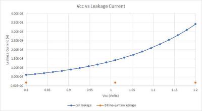
One of the main focuses of small-scale SRAM design is to achieve a balanced cell stability with optimized device sizing. However, there are a few challenges that need to be faced. One of these challenges is growing threshold voltage variations due to random dopant fluctuations. This can raise the sensitivity of status noise margin (SNM) to these process variations. Additionally, a mismatch in threshold voltage can lead to a mismatch in current on both halves of an SRAM cell. Generally, we want to prevent degradation of SNM, and we want the current on both halves to be identical. But we cannot dynamically change the threshold voltage of the sizing of these transistors. Power dissipation in SRAM circuits can be categorized into two main types - dynamic and static power dissipation. For static power dissipation, it is due to leakage current drawn from the power line. The main contributor of leakage current is the sub-threshold current. For SRAM, during idle phase, the workline (WL) is at WL=0 and two bitlines are precharged to BL=1, BLB=1. Thus there are two major leakage paths, 1) Cell Vcc to ground and 2) BL (BLB) to ground through the access transistor. Generally, the static power dissipation can be expressed as equation: Pstatict =VddIsube(Vgs -Vt)/nVth We can see the exponential increase of subthreshold leakage drain current with decreasing Vt for a given Vgs. This further proves that changing threshold voltage may lead to more negative impact on SRAM operation. In section II, we will discuss our proposed design and what this contributes to cell margins, stability, and leakage.
STATE OF THE ART & CONTRIBUTION
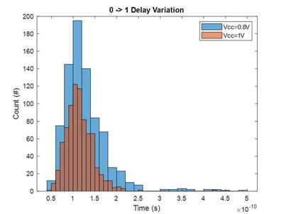
We propose dynamically switching between two voltage levels during read and write operations. In doing so, we can improve read and write margins independently without compromising each other. During write mode, we apply a supply voltage lower than the Word Line (WL) voltage. This weakens the pull-up network of the cell. During a read operation, we apply a supply voltage larger than the WL voltage. This strengthens the pull-down network which reduces read voltage and increases the trip point. Earlier research [1] has shown how margins can be improved using a dynamic power supply voltage. But they exclude Monte Carlo methodologies to find a relationship between supply voltage and average access delay. In this paper, we plan to confirm their key discoveries in margins and leakage power saving by conducting a waveform analysis on an SRAM schematic. Then, we propose designing an SRAM cell layout and conducting a Monte Carlo simulation to model a gaussian distribution of average access time. We then estimate read and write failures based on this distribution. The goal of this design is to improve margins, reduce access delay, and increase leakage power saving.
METHODOLOGY
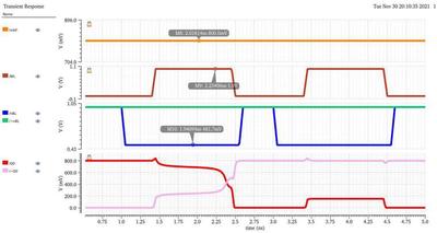
First, a schematic of an SRAM was created. Pfets were sized to 90 nm. Access transistors were sized to 135 nm. Nfets were sized to 180 nm. This cell was used for waveform analysis to measure the margins. To measure the write margin, The bit line (BL) voltage was sweeped to estimate the minimum voltage needed to create a transition at the storage node. To measure the read margin, we needed to find the difference between the trip point and the read voltage.
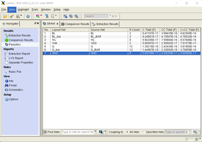
We then implemented a layout for one SRAM cell because layout will help us understand the intricate details of parasites.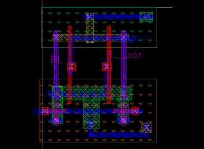
KEY FINDINGS
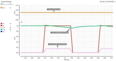
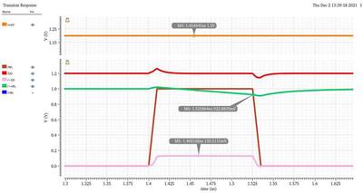
Using a standard 1.0V supply voltage, the write margin was measured to be 397mV. With a 800mV supply voltage, the write margin was measured to be 481mV. So, the write margin increased when we apply Vcc_Low. Two waveforms can be seen below that illustrate the waveform for this transient analysis.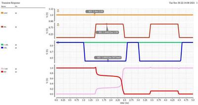
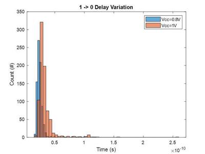
| Item | Write Margin | Read Margin | Monte Carlo Average Fall Delay | Monte Carlo Average Rise Delay |
|---|---|---|---|---|
| Baseline | 397.8 mV | 271 mV | 329.46 ps | 115.82 ps |
| Dynamic Vcc | 481.7 mV | 285 mV | 252.26 ps | 127.4 ps |
FUTURE WORK
In the future, we plan to expand our work from one cell to one bank (2kB). Our hope would be to integrate column-based power supply techniques to further improve cell stability. That way, we can test our functionality under a more complex scheme. In addition, we could further analyze leakage power saving for a more complete design.
References
[1] K. Zhang et al., “A 3-GHz 70MB SRAM in 65nm CMOS technology with integrated column-based dynamic power supply,” ISSCC. 2005 IEEE International Digest of Technical Papers. Solid-State Circuits Conference, 2005., 2005, pp. 474-611 Vol. 1, doi: 10.1109/ISSCC.2005.1494075. [2] 6T SRAM Cell Design, https://www.iue.tuwien.ac.at/phd/entner/node34.html E. Grossar, M. Stucchi, K. Maex and W. Dehaene, “Read Stability and Write-Ability Analysis of SRAM Cells for Nanometer Technologies,” in IEEE Journal of Solid-State Circuits, vol. 41, no. 11, pp. 2577-2588, Nov. 2006, doi: 10.1109/JSSC.2006.883344. [3] Tripti Tripathi , Durg Singh Chauhan, Sanjay Kumar Singh, “A Novel Approach to Design SRAM Cells for Low Leakage and Improved Stability,” Journal of Low Power Electronics and Applications [4] M. Mamidipaka, K Khouri, N Dutt, M. Abadir, “Leakage Power Estimation in SRAMs,” CECS Technical Report #03-32