A 12-bit Two-Stage Pipelined SAR ADC design
 Image credit: predictabledesigns.com
Overview
In this project, we designed a 2-stage pipelined Successive Approximation Register (SAR) Analog to Digital Converter (ADC). SAR ADC architectures are popular for achieving high energy efficiency but they suffer from resolution and speed limitations. The pipelined SAR architecture divides a moderate resolution SAR ADC into some low resolution SAR ADCs. The target specifications are given in the following table:
| Item | Specifications |
|---|---|
| Technology | 45nm (NCSU FreePDK45) |
| Power supply | VDD = 1.2V, VSS = 0V |
| Resistor size | < 100kΩ |
| Capacitor size | 2fF~ 10pF |
| ENOB@ Nyquist rate | >12bits |
| Sampling rate | >30MS/s |
| Walden figure-of-merit (FOM) | < 100-fJ/conversion-step |
Get Started
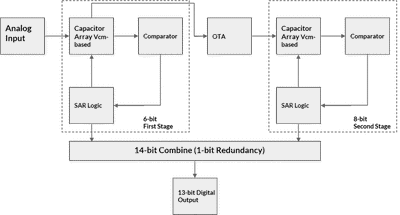
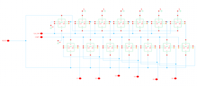
The diagram above shows the block diagram of the SAR ADC architecture. The ADC is a pipeline of a 6-bit and a 8-bit SAR ADCs. We decide to use differential sampling in order to cancel the common mode sampling offset. Furthermore, Vcm-based switching technique is used in both stages to lower the power consumption of the whole system.
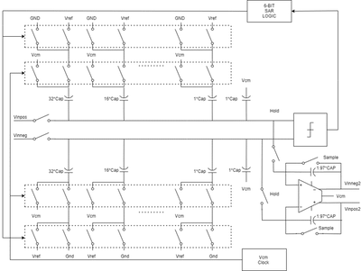
The first stage has 6-bit effective resolution. The first stage sub-ADC and CDAC share the same sampling capacitor array. There are several typical switching techniques that are available. We decide to use Vcm based switching technique mainly because the low power consumption and faster settling speed. However, one biggest drawback of this method is that it requires extra switches to control each capacitor. There are three possibilities at all sampling capacitors. Before the certain bit compared, the corresponding capacitor’s bottom plate is connected to Vcm. After comparison, its bottom plate will be connected to either ground or Vref depends on the comparing result is 1 or 0. Notice that the positive pair sampling capacitor array and the negative pair sampling capacitor array are connected opposite to each other. These sets of switches are controlled by a SAR logic unit which I’ll go over in next section. Additional independent clock sets are used to make sure each capacitor is in the right phase.
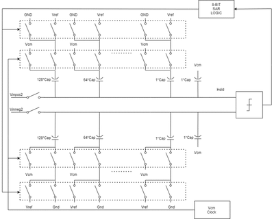
The second stage is a 8-bit SAR ADC. The use of SAR architecture in the second stage enables a large resolution in this single stage. The implementation is very similar compare to the first stage but has two more capacitor sets.
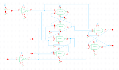
SAR Logic
| Clock | D1 | D2 | D3 | D4 | D5 | D6 | COMP. Out |
|---|---|---|---|---|---|---|---|
| RESET | 0 | 0 | 0 | 0 | 0 | 0 | – |
| 1 | 1 | 0 | 0 | 0 | 0 | 0 | D1 |
| 2 | D1 | 1 | 0 | 0 | 0 | 0 | D2 |
| 3 | D1 | D2 | 1 | 0 | 0 | 0 | D3 |
| 4 | D1 | D2 | D3 | 1 | 0 | 0 | D4 |
| 5 | D1 | D2 | D3 | D4 | 1 | 0 | D5 |
| 6 | D1 | D2 | D3 | D4 | D5 | 1 | D6 |
| 7 | D1 | D2 | D3 | D4 | D5 | D6 | – |
Below is the SAR Logic testing result. Notice that the input (Data) is set to 110000. Our SAR Logic output for each bit matches the input correctly.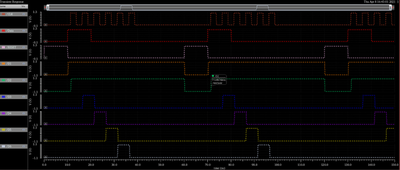
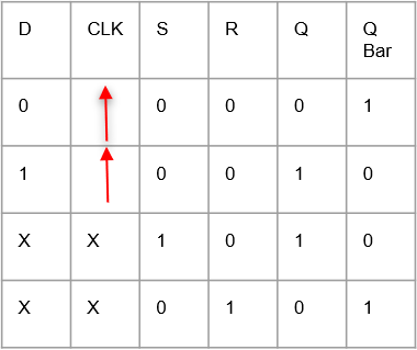
D Flip Flop
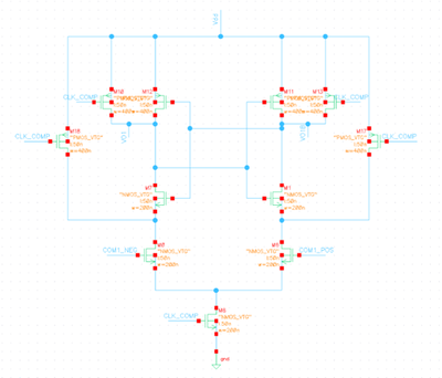
Comparator
License
Copyright Zhe Liu.