An AI accelerator can have enormous computing capability and still spend time waiting for data. Memory has to supply the inputs quickly enough to keep that hardware productive. High-Bandwidth Memory, or HBM, addresses this problem by combining stacked DRAM with a very wide interface close to the processor. Micron’s overview describes this data-delivery role as HBM’s central advantage.
What makes HBM different?
HBM stacks multiple memory dies vertically and connects them through through-silicon vias (TSVs). These are electrical connections that pass through the silicon. SK’s 2024 introduction explains how this architecture brings high data throughput into a compact footprint.
The stack is only part of the story. HBM sits beside the processor within an advanced package, commonly connected through an interposer. Short connections and many parallel data paths make it possible to move substantial amounts of data efficiently. Micron describes this combination of physical proximity and a wide interface in its HBM FAQ.
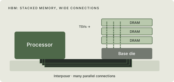
Conceptual illustration, not to scale. Individual implementations vary.
Bandwidth is a multiplication problem
Three terms help keep memory discussions precise:
- Capacity is how much data memory can hold.
- Bandwidth is how much data it can transfer per second.
- Latency is how long an individual access takes.
They describe different properties. More capacity does not automatically mean more bandwidth, and a high bandwidth specification does not promise low latency.
For a data interface, the theoretical peak is:
Bandwidth (GB/s) = data rate per pin (Gb/s) × data bus width (bits) ÷ 8
As an illustrative calculation, a 1,024-bit interface running at 9.6 Gb/s per pin yields 1,228.8 GB/s, or about 1.23 TB/s using decimal units. The input rate is already a transfer rate; it should not be doubled again.
This is a peak interface calculation, not a measured application result. It is useful for understanding why interface width matters, but it does not establish how much bandwidth a particular workload will sustain.
From HBM3E to HBM4
Samsung’s product page lists a 1,024-bit organization for HBM3E and 2,048 bits for HBM4. That wider interface gives HBM4 another way to increase throughput alongside higher per-pin rates. Samsung also describes its HBM4 implementation as combining DRAM with a logic base die manufactured on a 4 nm process.
Micron’s current portfolio lists more than 1.2 TB/s per stack for HBM3E and more than 2.8 TB/s for HBM4. These are manufacturer product claims, not universal specifications for every device in either generation.
When comparing numbers, check whether they describe one stack or an entire accelerator, which speed grade is being discussed, and whether the figure is theoretical or measured. Product pages and older explainers can describe different points in the technology’s evolution.
More bandwidth still has to fit inside a package
A wider interface requires more physical connections. A taller stack has to remain manufacturable and manageable thermally. These constraints are closely linked: SK hynix’s packaging research explicitly treats bandwidth, capacity, thermal behavior, stack height, TSV density, bonding pitch, and reliability as a combined optimization problem.
Heat remains a challenge as stacking and operating speeds increase. SK hynix’s iHBM announcement highlights thermal management as an active area of development.
My takeaway from these public descriptions is that an HBM specification is only one part of the engineering problem. The useful result is a memory system that can deliver its performance within the package’s electrical, thermal, and physical constraints.
Why HBM matters
HBM connects two parts of the AI performance story: processing data and delivering it. Its wide interfaces, compact stacks, and close integration with the processor make memory an architectural consideration from the beginning.
The question I find most useful is simple: can the system keep its compute resources supplied with data efficiently? HBM is one important answer—and its continued evolution shows how much progress depends on memory and packaging working together.
Reading further
The following five pages informed the reading for this post. Technical descriptions and product figures above are linked to manufacturer sources.
- SK — HBM Technology: The Silent Catalyst of the AI Revolution: a historical introduction from January 2024.
- Micron — High-bandwidth memory: product information and architectural FAQs.
- Samsung — HBM: generation-specific product information.
- IONOS — What is High Bandwidth Memory?: an accessible overview for additional background.
- SemiAnalysis — Scaling the Memory Wall: industry analysis of manufacturing and architectural tradeoffs. The report is marked paid; only the publicly accessible material was reviewed.
Product-page details checked November 10, 2026. Product claims and availability can change.